


How to Design a Chip

By Charlie Kidd │ ICM HPQC Fund │ October 2026
“Written by humans, please don’t blame the robots for our typos”
Modern chip designs are arguably one of the greatest feats of engineering ever achieved. Over the last few decades, electrical engineers have designed chips with ever increasing numbers of transistors, which are the tiny switches that drive almost all modern computation.
The latest NVIDIA Rubin graphics processing unit (GPU) has 336 billion of them.1 For context, that’s roughly as many stars as are in the Milky Way, or as many hairs on the heads of every single person in Mongolia, or as many keys as there are on 3.8 billion pianos. In short, a staggering amount, packed onto the same area as four £1 coins.
The result is an astonishing increase in the amount of processing power available to us in our devices. For example, a modern smartphone has well over 100,000 times the processing power of the computer that guided Apollo 11 to the Moon.2
Given this level of complexity, how do our (not so) humble engineers accomplish such a design feat? How does an idea become a blueprint for a computer chip? Who is doing interesting things in this space? And how is AI disrupting the process that enabled its creation?
Read on, and all will be revealed.
Some basics before we begin (only if you need)
If, like me, you’ve not got a PhD in computer science, a quick primer may help. If you’re familiar with computer science, skip this part.
The core technology that makes chips work is the transistor. These are tiny switches that, in modern computers, generally have two states – on or off – which are assigned numerical values of 1 or 0. Many transistors are connected into a circuit, allowing them to work together to perform ‘logical functions’ – like adding, subtracting, multiplying and dividing.
Put enough circuits together and it creates a chip capable of the complicated maths and logic that power most useful functions in your devices, from the banker’s spreadsheets to the musician’s digital recordings.
Chips are usually made of silicon because it is abundant, relatively cheap, and its electrical properties can be precisely controlled. Gordon Moore, the co-founder of Intel, famously predicted in the 1960s that the number of transistors that could be fitted onto a chip would double every year. This was later revised to every two years and was dubbed ‘Moore’s Law’.
Despite being a prediction rather than a law of nature, it proved remarkably accurate for decades, although the traditional pace of scaling has slowed more recently.3,4

As technology has improved, demand has skyrocketed. The semiconductor market grew from $139bn in 2001 to almost $796bn in 2025, with demand exploding in tandem for all of the materials, manufacturing capacity and expertise required to make them.5,6

The biggest chip companies are amongst the most famous and valuable organisations in the world. Crucially, most do not manufacture their own chips. Instead, they design them and send the blueprint off to a foundry - often TSMC in Taiwan - which manufactures the physical chip in a fabrication plant, or ‘fab’.
Hence these companies are known as ‘fabless’ (see the name of this exquisite publication).
For much of the industry, it is therefore the design process and intellectual property behind it that create much of the value.7
A game of trade-offs
So what is the actual process of designing one of these golden blueprints?
Like most engineering challenges, every step in the design process presents conflicting goals for the engineer to consider. Just as you might trade integrity for credibility when you tell your book club you finished the reading, engineers have to make trade-offs too.
These decisions are mostly captured in three letters, PPA, which stands for power, performance and area. You normally cannot optimise all three at once. A faster design may consume more power; reducing power may require more silicon; squeezing the design into less area may constrain performance.

PPA isn’t the whole story. Designers also care about cost, yield - what proportion of the manufactured chips work - reliability, time-to-market and how specialised the chip should be.
But PPA gives us a useful scoreboard to keep in mind as we work through the design process.
And this process is really (really) hard. Designing a cutting-edge chip can take two to three years, involve hundreds of engineers and require countless iterations before a design is finally ready for manufacturing.8 A mistake at any stage, that is not caught quickly, can therefore be eye-wateringly expensive.
Why does it take so long? A many-step process (but we’re going to distil it to five)
The journey from an idea to working silicon can be captured in five core steps.9
1. Specification & Architecture. What should the chip actually do? Engineers decide its functions, architecture and targets, including our PPA trade-offs.
2. Register-transfer level (RTL) Design & Verification. Engineers describe the intended digital logic in code, then repeatedly simulate and test it to establish that it behaves correctly.
3. Synthesis & Physical Implementation. Software converts that abstract logic into a network of logic gates (small circuits that perform basic logical operations), then works out where those gates and the wires connecting them should physically sit on the chip.
4. Sign-off & Tape-out. The team checks that the finished design meets requirements for power, manufacturing and timing - whether signals arrive quickly enough. Once everyone is satisfied, the final blueprint is sent to the fab for manufacturing. This is known as ’tape-out’.
5. Fabrication, Test & Validation. The fab turns the blueprint into silicon. The first chips are packaged, tested and powered up to establish that the physical device works as intended.
Before much of this can happen, the designer has to know how the chip will actually be manufactured. A foundry such as TSMC provides a Process Design Kit, or PDK, which is essentially a set of rules, models and building blocks designers need to create something that its manufacturing process can actually make. It’s a little like a kitchen telling you what cooking equipment it has before you write the recipe.

Getting the right tools for the job
In the early days, chip designs were literally laid out by hand. But billions of transistors? Luckily someone came up with software tools to prevent chip engineers from getting carpal tunnel. This is known as Electronic Design Automation, or EDA.
The global EDA software market was worth an estimated $14.9bn in 2025, and is forecast to reach $35.6bn by 2034, growing at around 10% a year. It is also highly concentrated, with three companies – Synopsys, Cadence and Siemens – together controlling around three-quarters of the market. Industry data shows EDA, semiconductor IP and design-services revenues of $5.5bn in Q4 2025 alone, up 10.3% year-on-year.10,11,12

The first important thing to understand is that EDA is not one piece of software.
A chip engineer does not open ‘Cadence’, design a chip and press save. EDA is more like a very large, specialised software toolbox, with different programs used for different stages of the design process. A modern chip can pass through dozens of tools, often supplied by several different companies, before it is ready to manufacture.13
Some tools are essentially sophisticated coding and testing environments. Engineers writing the RTL we met earlier use software to simulate what that code will do, find bugs and check that the resulting hardware behaves as intended.
This matters because finding a bug on a laptop is considerably cheaper than discovering it after manufacturing. Companies therefore spend enormous amounts of time and money proving their designs work before producing any silicon.
Other tools do the heavy lifting of turning the design into its physical form. Software such as Synopsys Fusion Compiler or Cadence Innovus helps decide how millions or billions of circuit elements should actually be arranged and connected.
Another collection of tools checks the result. Cadence Tempus and Synopsys PrimeTime, for example, analyse whether signals will arrive at the right places quickly enough, while Siemens’ Calibre checks whether the eventual layout complies with the foundry’s manufacturing rules.13,14,15,16

This specialisation is part of what makes EDA such an interesting software market. These are not interchangeable b2b SaaS productivity apps. A particular tool may contain decades of accumulated semiconductor know-how, have been qualified against manufacturing processes at the world’s leading foundries, and be deeply embedded in a chip company’s own internal workflows. Engineers build scripts, data and processes around these tools over years.
The different suppliers are therefore both competitors and, slightly awkwardly, forced collaborators. A company might use one vendor’s software to simulate a design, another’s to lay it out, and a third’s to check it before manufacturing.
The output of one tool therefore has to feed reliably into the next. Over time, the largest EDA companies have expanded their suites, seeking to control more of the workflow around the chip design process.
EDA companies also sell something else that makes this process considerably easier: intellectual property, or IP blocks.
There is little point in designing common functions from scratch when they are needed across many different chips, whether that’s a processor core or the standard connections that allow a chip to communicate with other devices.
Designers can instead license pre-designed and pre-verified blocks and integrate them into a larger chip - a little like using an existing software library rather than rewriting every function from scratch.
The result is that modern chip design is already, to a remarkable extent, a software-mediated process.
Engineers still decide what should be built, make the architectural choices and ultimately take responsibility for whether the design works. But supporting those decisions is an enormous collection of highly specialised software performing simulation, verification, optimisation and physical design, with much of it supplied by just three companies.
So if software already does so much of the work involved in designing a chip, what happens when that software gets substantially more intelligent?
Can AI help, and is data king?
I’ve managed to get this far without using the phrase “AI” (impressive), but all good things must come to an end. With advances in AI and other high-performance computing use cases, even more ambitious chip architectures are in the works. These include packing even more transistors onto individual chips, combining multiple chips together, and creating 3D architectures with multiple chip components, and more. All of this adds complexity to an already mind-blowingly complicated process.17

Enter agentic AI. These are AI systems that can plan a task, use software tools and execute multiple steps towards a goal before checking their own work and continuing on. As with many industries, there is much discussion about how it will impact the chip design process.
But, of course, there’s no such thing as a free lunch (unless you work at Google), meaning the EDA industry has its own unique challenges to deploying AI agents. Most importantly, you’ve got to find the data to train your models. And who actually has it?
Mostly the chip designers themselves. Every chip comes with its design code, the code used to test it, a history of bugs and plenty of internal documentation. Much of this is highly confidential.18 For a sense of scale, when NVIDIA adapted an AI model for its engineers, it used about 23 billion tokens (think chunks of words or code) of internal data.19
Foundries hold the manufacturing side of the equation and generally release their PDKs only under strict confidentiality agreements.20 As a result, very little chip design data is publicly available.21
One group of academics estimates that the total amount of public design data available is ‘many orders of magnitude smaller’ than the data used to train general language models.22
Then again, the big LLMs were trained on pretty much the entire internet, so… maybe that’s not surprising. It’s also not clear whether the data in its existing format would even be effective for model training anyway.23

How much data an AI model needs depends on what you’re asking it to do. Traditional training methods can of course be very data hungry. One study estimates that specialised RTL models need at least 100 million examples of code and labels to perform well,23 well beyond what’s publicly available.
A giant like NVIDIA, though, has enough of its own to tailor an existing model to its work, for only 1.5% or so of the computing cost of training the original generalist model.19
Reinforcement learning is another way of training models, and plays a different part in our story. It learns by trial and error against a simulation, so it needs far fewer past designs. AlphaChip, Google’s chip layout system, was pretrained on just 20 chip blocks24 and has been used in the last three generations of its TPU chips.25
The catch is that reinforcement learning still needs plenty of computing power, plus tools or simulators to learn against, which the model can learn. Many of these tools come from the three EDA incumbents.

What about the EDA vendors? They do see some customer data, but it’s walled off. Synopsys stores proprietary information belonging to its customers,14 but vendors serving several clients have to keep that work compartmentalised to prevent leaks.22
They therefore can’t simply pool everyone’s designs into one big training set. Instead, their AI products are set up to work with each client’s data separately. What the incumbents do hold outright is their design IP, such as the processor and connection blocks they license to chipmakers,14 plus unrestricted access to their own tools, which can be used to generate training data.23
Uptake of these tools is a rocky road
Even if you do manage to get hold of the data to train your models, some of the biggest chip players are saying that they are very apprehensive about letting agents in particular roam free in their secure environments during the design process (heard of Hugging Face?).26
Some of the risks can be handled with familiar measures like models that run on the customer’s premises, encryption, and promises not to train on customer data.22,27
Agents are harder. An agent that can run tools and scripts inside a design environment can be hijacked by instructions hidden in the material it reads. OpenAI itself says this kind of attack is “unlikely to ever be fully ‘solved’”.28
The standard response is to limit what an agent is allowed to do,29 which clearly doesn’t sit too well with the idea of agents autonomously running large chunks of the design process.
Then there’s the ‘black box’ nature of many models, where you can’t always trace exactly how an AI model arrived at an output, which is an issue for engineers for whom accountability, reliability and process knowledge are absolutely key.30
Chip design is also an expensive place to make mistakes. Only 14% of custom chip projects worked the first time in 2024, the lowest figure in more than twenty years, while a single set of manufacturing masks at the most advanced nodes costs tens of millions of dollars.31
Engineers therefore want proof before they trust a new tool, and even after adoption, as Siemens EDA’s Dan Yu put it, “we still have to do the quality check”.32 This cautions how EDA software is bought.
Cadence describes its sales cycle as “generally long, requiring up to six months or longer”, including on-site customer evaluations,13 while Synopsys points to “a substantial customer evaluation and approval process”.14
For a startup asking engineers to trust an AI that may not be able to fully explain its decisions, the path to adoption could be a long road.
None of these issues are likely to kill AI in EDA, but they’ll probably slow uptake, which anyway is happening at a variable rate across different types of workloads. For example, RTL creation, verification, testbench creation (the code used to test a design) and debugging are moving faster, since work can be generated and then checked relatively quickly against existing tools.17,33,34,35

Who’s playing part 1 – the incumbents
Given both the opportunity for change and the size of the market opportunity here, who are the key players? We’ll start with the incumbents, who are themselves moving fast to deploy AI in their products.
Each of the big three grew up around a different part of the design process, which still shapes what they’re known for.
Synopsys made its name automating the step that turns code into logic gates,36 and today covers most of the journey for a large digital chip, from testing the code through to the final layout. It also sells what it calls the broadest portfolio of IP blocks, and in July 2025 it bought Ansys, adding software that simulates how a chip behaves physically, including how power flows through it.14
Cadence’s flagship is Virtuoso, used to design analogue circuits that handle real-world signals. It is also strong in digital chip layout, hardware used for test designs before manufacturing, and the design of packages and circuit boards - increasingly important as chips become stacks of smaller chips.13
Siemens (formerly Mentor Graphics) is best known for Calibre, which checks that a finished layout obeys the foundry’s manufacturing rules. It was the first tool foundries wrote their rules for,37 and Siemens also has tools that make chips easier to test once they’ve been made.38
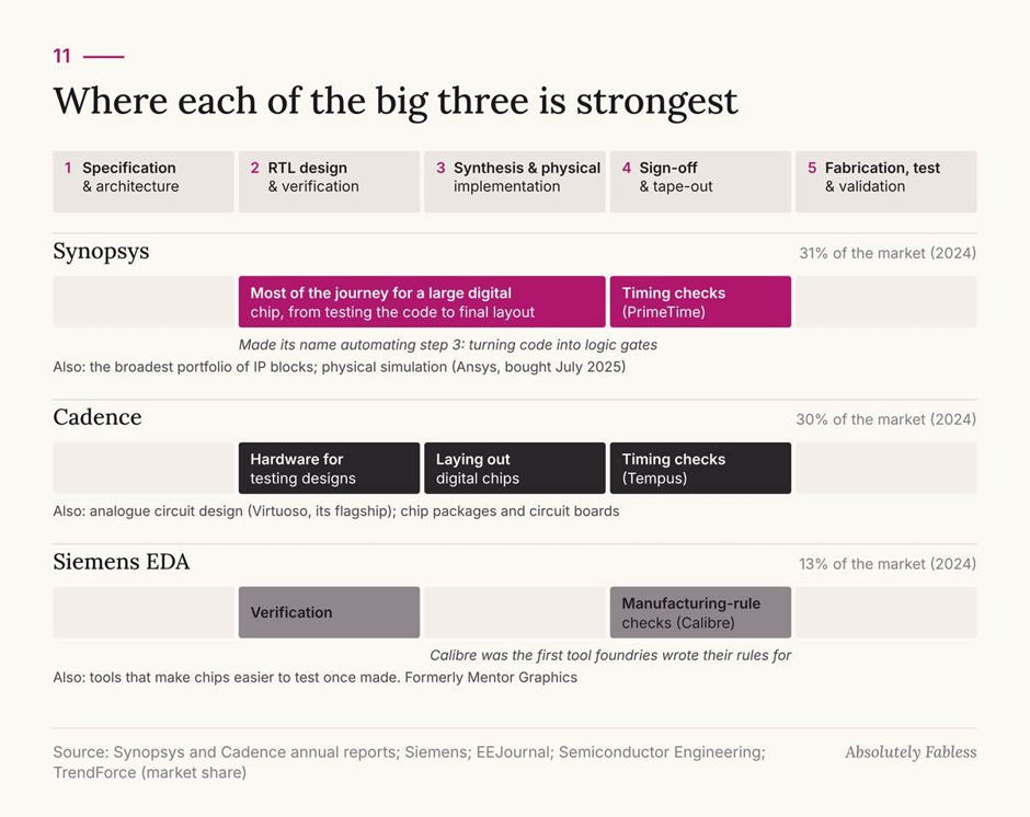
Why pick one over another? In practice, many customers choose tool by tool and use more than one vendor.13 Trust matters a lot here. Calibre has held its lead for decades partly because foundries, and their customers, stick with the verification tools they trust.37
Synopsys identifies technology, quality, ease of use, licence terms, price, support, flexibility and interoperability as factors customers consider.14
The way tools are sold also makes switching difficult. Cadence licences generally run for two to three years and cover the products in the deal from day one.13 When a rival (or a startup) comes knocking, the customer may already have paid for the incumbent’s product and built its workflow around it.

Who’s playing part 2 – the startups
So, startups aren’t just competing with big fish with deep pockets. The incumbents already own much of the underlying toolchain, have decades-long customer relationships and sit on enormous amounts of domain knowledge.
The question is whether AI reinforces those advantages, or whether the technology creates such a different way of designing chips that a new entrant can establish a new position in the toolchain.
The incumbents’ AI plans follow their traditional expertise, with agents sitting on top of their existing tools. That means the point where a startup enters the process can determine which giant it’s up against. An analogue layout startup is rolling its tanks onto Cadence’s home turf, while one that checks designs against manufacturing rules is up against Calibre. Startups that operate across all three vendors’ tools go head to head with all of them, but may also fit more naturally with the way customers already work.
Roughly speaking, three different types of challengers are emerging.
1. Target a particularly painful part of the existing process. Silimate is going after front-end debugging and PPA optimisation, Astrus is focused on analogue layout, while others are targeting verification or physical design.
2. Sit above the existing EDA toolchain. Use agents to operate tools that engineers already use, effectively automating more of the workflow without replacing the underlying machinery. Agentrys is perhaps the clearest example.
3. Rethink the design process itself. Build models that operate across much more of the toolchain, potentially dispensing with the traditional EDA design process altogether. Ricursive is pursuing this broader vision.


It is far too early to know which approach wins, and they aren’t necessarily mutually exclusive. But they make for rather different venture bets. Companies targeting individual problems potentially have the easiest route into customers since they can address a clear pain point without asking a design team to replace its existing toolchain.
Orchestration companies can leave the underlying tools in place while gradually automating more of the workflow. The challengers spanning the full process have the biggest ambition – and potentially the largest prize – but also have to overcome the biggest barriers in trust, integration and accumulated engineering knowledge.
So what do we think? Who’s going to win?
So does whoever holds the data win? We don’t think it’s that simple. The richest data sits with the big chip designers, who in our view are more likely to use it to speed up their own engineers than to sell tools to their competitors.
That creates a risk for startups, since their biggest potential customers may decide to do the job themselves. It also puts EDA incumbents and startups in the same boat. To learn from a client’s designs, you have to work inside the client’s environment.
Reinforcement learning and physics-based simulation offer ways to sidestep some of this, although performance remains uncertain and the compute for training is expensive. The EDA incumbents are also able to get around this in some cases where they own and license IP themselves.
The big chip designers face the age-old challenge of not being as agile or focused as a startup. And they have outsourced the development of EDA tools for decades, so they don’t have the same in-house expertise as Synopsys, Cadence and Siemens.
So where might the balance of power ultimately settle? f I were a betting man, I would suggest that:
Big chip designers win if they are able to move quickly, leverage their proprietary knowledge base and attract the right talent, - all for less than it would cost to buy tools externally. That’s not easy, so my bet isn’t on them.
The big EDA incumbents win if they can move quickly enough, access sufficient training data, and make AI a genuine organisational priority. This is also not easy, but I would argue it’s much more doable than scenario 1.
Startups win if they can outmanoeuvre the big firms through raw focus, technical excellence, attracting top talent, and moving fast. I think there are some highly promising possibilities here, so it’s a space to watch. Over time, the really important question is whether they are simply making the incumbent tools easier to use, or accumulating enough proprietary data, workflow knowledge and customer trust to become a genuinely defensible part of the toolchain themselves.
A major venture-scale return over the long term may rely on large-scale displacement of the incumbents rather than incremental improvements. I’d be particularly bullish about companies getting around the data access issues, such as those deploying reinforcement learning.
Taking on the big players is no easy task, and claims of disruption should be treated with a healthy balance of admiration and scepticism. However, EDA has seen successive waves of new tools and vendors as chip-design methodologies have evolved over the past 60 years (see the timeline below).
Importantly, the market is also big enough for multiple winners.

So, when meeting an early-stage venture in this space, I would ask the following questions:
· How are you training your models, and who owns the data?
· Do you augment or replace incumbents?
· Where does your product sit in the workflow? How much of the full process will it be able to execute?
· What’s your differentiation compared to other companies in this space?
If you’re founding, investing, or just plain interested in this area, please drop me a message on LinkedIn, our website or via Substack. And tell me where I’m wrong!

Charlie Kidd
Head of Origination, ICM HPQC Fund
ICM Global Funds Pte Ltd
October 2026
Sources:
1. NVIDIA, “Inside NVIDIA Rubin GPU Architecture: Powering the Era of Agentic AI” (21 July 2026). https://developer.nvidia.com/blog/inside-nvidia-rubin-gpu-architecture-powering-the-era-of-agentic-ai/
2. World Economic Forum, “Why your iPhone is more powerful than the computer that landed Apollo 11 on the moon” (2 July 2019). https://www.weforum.org/stories/2019/07/one-small-step-for-man-one-giant-leap-for-your-mobile-phone/
3. Intel, “Moore’s Law” (18 September 2023). https://www.intel.com/content/www/us/en/newsroom/resources/moores-law.html
4. Hennessy and Patterson, “A New Golden Age for Computer Architecture”, Communications of the ACM (February 2019). https://cacm.acm.org/research/a-new-golden-age-for-computer-architecture/
5. EE Times, “Chip sales shrunk 32 percent to $139B in 2001, SIA says” (4 February 2002). https://www.eetimes.com/chip-sales-shrunk-32-percent-to-139b-in-2001-sia-says/
6. World Semiconductor Trade Statistics, “Global Semiconductor Market grows 26% in 2025 to $796B” (6 March 2026). https://www.wsts.org/76/103/Global-Semiconductor-Market-grows-26-in-2025-to-796B
7. TSMC, “TSMC Says IC Industry Success Starts with Design Collaboration” (14 April 2004). https://pr.tsmc.com/english/news/1287
8. Semiconductor Engineering (Karen Heyman), “AI’s Role In Chip Design Widens, Drawing In New Startups” (29 August 2024). https://semiengineering.com/ais-role-in-chip-design-widens-drawing-in-new-startups/
9. Synopsys, “What is ASIC Design? – How it Works” (31 July 2025). https://www.synopsys.com/glossary/what-is-asic-design.html
10. Fortune Business Insights, “Electronic Design Automation Software Market Size, Share & Industry Analysis, Forecast to 2034” (accessed 7 October 2026). https://www.fortunebusinessinsights.com/electronic-design-automation-software-market-105985
11. TrendForce, “China Revenue at Risk as U.S. Curbs Slam EDA Giants: Impact on Synopsys, Cadence and More” (2 June 2025). https://www.trendforce.com/news/2025/06/02/news-china-revenue-at-risk-as-u-s-curbs-slam-eda-giants-impact-on-synopsys-cadence-and-more/
12. SEMI, “ESD Alliance Reports Electronic System Design Industry Posts $5.5 Billion in Revenue in Q4 2025” (13 April 2026). https://www.semi.org/en/semi-press-release/esd-alliance-reports-electronic-system-design-industry-posts-5.5-billion-dollars-in-revenue-in-q4-2025
13. Cadence, “Annual Report on Form 10-K for fiscal year 2025” (2026). https://www.sec.gov/Archives/edgar/data/813672/000081367226000016/cdns-20251231.htm
14. Synopsys, “Annual Report on Form 10-K for fiscal year 2025” (2025). https://www.sec.gov/Archives/edgar/data/883241/000088324125000028/snps-20251031.htm
15. Cadence, “Tempus Timing Solution”. https://www.cadence.com/en_US/home/tools/digital-design-and-signoff/silicon-signoff/tempus-timing-signoff-solution.html
16. Siemens, “Calibre nmDRC”. https://www.siemens.com/en-gb/products/ic/calibre-design/physical-verification/design-rule-checking/
17. Synopsys, “What is Electronic Design Automation (EDA)?”. https://www.synopsys.com/glossary/what-is-electronic-design-automation.html
18. Pan et al., “Towards Collaborative Intelligence: Routability Estimation based on Decentralized Private Data”, Design Automation Conference (2022). https://arxiv.org/abs/2203.16009
19. Liu et al. (NVIDIA), “ChipNeMo: Domain-Adapted LLMs for Chip Design” (2023). https://arxiv.org/abs/2311.00176
20. Stony Brook University, “Using Process Design Kits (PDKs) in Research”. https://www.stonybrook.edu/research-security/research_activities/pdk.html
21. Calzada et al., “VerilogDB: The Largest, Highest-Quality Dataset with a Preprocessing Framework for LLM-based RTL Generation” (2025). https://arxiv.org/abs/2507.13369
22. Xu et al., “Revolution or Hype? Seeking the Limits of Large Models in Hardware Design”, ICCAD (2025). https://arxiv.org/abs/2509.04905
23. Chang et al., “Data is all you need: Finetuning LLMs for chip design via an automated design-data augmentation framework”, Design Automation Conference (2024). https://arxiv.org/abs/2403.11202
24. Mirhoseini et al., “A graph placement methodology for fast chip design”, Nature (9 June 2021). https://www.nature.com/articles/s41586-021-03544-w
25. Google DeepMind, “How AlphaChip transformed computer chip design” (26 September 2024). https://deepmind.google/blog/how-alphachip-transformed-computer-chip-design/
26. OpenAI, “The Hugging Face incident and the road ahead” (26 August 2026). https://openai.com/index/hugging-face-incident-and-the-road-ahead/
27. Synopsys, “OpenAI and Synopsys Announce GPT-Synopsys Frontier Intelligence to Revolutionize Chip Design” (30 September 2026). https://www.synopsys.com/ja-jp/japan/press-releases/2026-09-30-openai-and-synopsys-announce-gpt-synopsys-frontier-intelligence-to-revolutionize-chip-design.html
28. OpenAI, “Continuously hardening ChatGPT Atlas against prompt injection attacks” (22 December 2025). https://openai.com/index/hardening-atlas-against-prompt-injection/
29. National Cyber Security Centre, “Prompt injection is not SQL injection (it may be worse)” (8 December 2025). https://www.ncsc.gov.uk/blog-post/prompt-injection-is-not-sql-injection
30. National Institute of Standards and Technology, “AI Risks and Trustworthiness”, AI Risk Management Framework, section 3. https://airc.nist.gov/airmf-resources/airmf/3-sec-characteristics/
31. Siemens EDA, “Why First-Silicon Success Is Getting Harder for System Companies” (3 September 2025). https://blogs.sw.siemens.com/verificationhorizons/2025/09/03/why-first-silicon-success-is-getting-harder-for-system-companies
32. Semiconductor Engineering, “AI Adoption Slow For Design Tools” (1 May 2023). https://semiengineering.com/slow-ai-adoption-within-eda
33. Cadence, “The Autonomous Chip-to-System Engineer Has Arrived” (26 July 2026). https://community.cadence.com/cadence_blogs_8/b/corporate-news/posts/the-autonomous-chip-to-system-engineer-has-arrived
34. Synopsys, “Synopsys Powers Autonomous Engineering with a Broad Portfolio of Long-Horizon Agents and Autopilot Platform” (28 September 2026). https://news.synopsys.com/2026-09-28-Synopsys-Powers-Autonomous-Engineering-with-a-Broad-Portfolio-of-Long-Horizon-Agents-and-Autopilot-Platform
35. ChipAgents, “Newsroom”. https://chipagents.ai/newsroom
36. EEJournal, “A Brief and Personal History of EDA, Part 4: Cadence, Synopsys, and Mentor Graphics – The EDA Era” (15 April 2024). https://www.eejournal.com/article/a-brief-and-personal-history-of-eda-part-4-cadence-synopsys-and-mentor-graphics-the-eda-era/
37. Semiconductor Engineering, “Calibre Evolves Constantly” (11 May 2017). https://semiengineering.com/calibre-evolves-constantly/
38. Siemens, “Electronic Design Automation (EDA)”. https://www.siemens.com/en-us/technology/electronic-design-automation-eda/
39. Siemens, “Siemens launches Fuse EDA AI Agent for automation across semiconductor, 3D IC and PCB system workflows” (16 March 2026). https://news.siemens.com/en-gb/siemens-fuse-eda-ai-agent/
40. Silimate, company website. https://www.silimate.com/
41. PitchBook, Silimate company profile, accessed 30 September 2026.
42. Astrus, company website. https://www.astrus.ai/
43. Fasken, “Astrus closes US$12 million Series A financing” (September 2026). https://www.fasken.com/en/experience/2026/09/astrus-closes-us12m-series-a-financing
44. EE Times, “Startup Wants to Speed Up Chip Design With AI in RTL to GDSII Path” (26 February 2026). https://www.eetimes.com/startup-wants-to-speed-up-chip-design-with-ai-in-rtl-to-gdsii-path/
45. Business Standard, “Tattvam AI raises $1.7 million to speed up semiconductor chip design” (26 February 2026). https://www.business-standard.com/companies/start-ups/tattvam-ai-raises-1-7-million-to-speed-up-semiconductor-chip-design-126022600775_1.html
46. Agentrys, “Agentrys Raises $24.5 Million to Build Agentic Design Automation for Chipmakers” (26 August 2026). https://agentrys.ai/news/agentrys-raises-24-5-million
47. Cognichip, “ACI Enterprise – Artificial Chip Intelligence” (2026). https://www.cognichip.ai/
48. Cognichip, “Seligman Ventures Leads Cognichip’s $60M Series A to Back Physics-Informed AI for Chip Design” (1 April 2026). https://www.cognichip.ai/news/seligman-ventures-leads-cognichips-60m-series-a-to-back-physics-informed-ai-for-chip-design-intel-ceo-lip-bu-tan-and-seligman-ventures-umesh-padval-join-the-board
49. EE Times, “Startup Ricursive to Create an End-to-End AI Model for Chip Design” (10 June 2026). https://www.eetimes.com/startup-ricursive-to-create-an-end-to-end-ai-model-for-chip-design/
50. PR Newswire, “Ricursive Intelligence Raises $300 Million Series A at $4 Billion Valuation to Accelerate AI-Driven Semiconductor Design” (26 January 2026). https://www.prnewswire.com/news-releases/ricursive-intelligence-raises-300-million-series-a-at-4-billion-valuation-to-accelerate-ai-driven-semiconductor-design-302670061.html
Important Note:
The information in this article should not be considered an offer or solicitation to deal in the ICM HPQC Fund (Registration number T22VC0112B SF003) or ICM HPQC Fund 2 (Registration number T22VC0112B SF007) (the “Sub-funds”). The information is provided on a general basis for informational purposes only and is not to be relied upon as investment, legal, tax, or other advice. It does not take into account the investment objectives, financial situation, or particular needs of any specific investor. Investors should seek relevant professional advice before making any investment decision. The information presented has been obtained from sources believed to be reliable, but no representation or warranty is given or may be implied that it is accurate or complete. The Investment Manager reserves the right to amend the information contained herein at any time, without notice. Investments in the Sub-funds are subject to investment risks, including the possible loss of the principal amount invested. All forms of investments carry risks, including the risk of losing all of the invested amount. Investors should read the prospectus before deciding whether to acquire the units in the Sub-funds. The value of investments and the income derived therefrom may fall or rise. Past performance is not indicative of future performance. This document is intended solely for institutional investors and accredited investors as defined under the Securities and Futures Act 2001 of Singapore. The whole or any part of this work may not be reproduced, copied or transmitted or any of its contents disclosed to third parties without ICM Global Fund’s express written consent. This advertisement or publication has not been reviewed by the Monetary Authority of Singapore.
ICM HPQC Fund and ICM HPQC Fund 2 are registered Sub-Funds of the ICMGF VCC (the VCC), a variable capital company incorporated in the Republic of Singapore. The assets and liabilities of ICM HPQC Fund and ICM HPQC Fund 2 are segregated from other Sub-Funds of the VCC, in accordance with Section 29 of the VCC Act.
Get to know us better:




Comments